Clock Skew and TOF Circuit Model Diagram
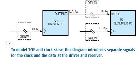
Engineering diagram designed to model Time of Flight (TOF) and clock skew by separating clock and data signal paths between driver and receiver. This technical reference helps engineers diagnose latency and signal synchronization issues in high-speed digital designs[cite: 778, 822].